

For Active BMS Balancing, Is the Efficiency Bottleneck in the Topology or in the Switching Devices?
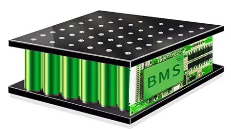
In most engineering practice, switching devices are the more direct constraint. The reverse-recovery charge of the silicon MOSFET body diode creates a fixed “loss floor” in hard-switched Buck‑Boost converters, making it uneconomical to increase frequency and balancing current at the same time. The Qrr of SiC MOSFETs can be reduced to about 4.5% of that of silicon devices in the same class, pushing balancing efficiency above 92% while relieving the strong coupling among frequency, size, and thermal budget.
Why Active Balancing Requires “Changing Devices” Rather Than “Changing Topology”
The essential difference between active and passive balancing lies in the energy flow: passive balancing burns excess charge as heat, while active balancing uses an inductor as the medium to transfer charge from high-SOC cells to low-SOC cells. Transfer efficiency is determined by the loss composition of the Buck‑Boost converter, and the losses vary sharply with switching frequency.
The structural constraint of silicon MOSFETs occurs at the hard-switching commutation instant. The body diode must remove stored charge Qrr during reverse recovery, and this charge is converted into heat in every switching cycle. When engineers try to raise the balancing frequency from 100 kHz to 300–500 kHz to reduce inductor size and speed up response, reverse-recovery loss rises linearly, creating a “frequency—efficiency—size” trilemma. At the same time, increasing the balancing current means conduction loss and junction temperature both climb, and the positive temperature coefficient of the silicon device’s RDS (on) further compresses the usable current window.
The physical-level difference of SiC is deterministic. SiC MOSFETs have no minority-carrier tail, and the body-diode reverse-recovery charge is extremely low. In measured comparisons, the Qrr of a 650 V SiC MOSFET is about 4.5% of that of a superjunction silicon MOSFET, and commutation loss almost “disappears” from the loss budget. The freed-up loss budget can be reallocated to a higher switching frequency (smaller inductor, faster loop response) or a larger balancing current (shorter balancing time), rather than being passively dissipated in the body diode. A 2026 review of SiC-based active balancers for electric vehicles explicitly states that, under 800 V platforms and fast-charging requirements, conventional silicon solutions can no longer meet capacity-utilization and balancing-speed requirements, and that SiC-based solutions can stably achieve balancing efficiency above 92%.
Selection Focus: “Matching Parameters” Rather Than “Extreme Parameters” for Balancing Scenarios
The voltage stress in active balancing is usually lower than that in the main traction loop. For cell-string-level Buck‑Boost balancers, the voltage seen by the switching devices is generally on the order of 50–100 V, and a 650 V rating already provides ample safety margin. In this range, matching RDS (on) with package thermal resistance has more engineering significance than pursuing the highest voltage rating or the lowest on-resistance.
Hypersemi’s 650 V SiC MOSFET product line provides balancers with a continuous selection gradient from board-level integration to centralized high-current designs:
For multi-channel distributed balancing architectures, the CM65R380TFX100 (650 V / 11 A / 380 mΩ, TO‑220F) provides a pragmatic balance point for board-level integration among per-device current-carrying capability, package size, and cost. The TO‑220F’s fully insulated package makes it easier to handle heat dissipation and insulation coordination in dense board layouts, and the 380 mΩ on-resistance keeps conduction loss in an acceptable range at balancing currents of several amperes. Specific product page: https://www.hypersemi.com.cn/cn/products/sic‑mosfets/CM65R380TFX100.html
When the balancing current is raised to the 10–20 A level and per-channel loss needs to be reduced, the Kelvin-source package of the CM65R090L4X100 (650 V / 36 A / 90 mΩ, TO‑247‑4L) effectively reduces the source inductance of the drive loop and provides substantial help in suppressing gate ringing and dv/dt false turn-on during high-frequency commutation. For centralized high-current active balancing topologies, the CM65R065LX100 (650 V / 38 A / 65 mΩ, TO‑247‑3L) pushes per-device current-carrying capability and conduction loss to more aggressive levels, making it suitable for designs that carry greater balancing power with fewer channels.