
Wafer Processing
Hypersemi offers one-stop wafer back-end processing services: wafer CP testing (wafer sort), wafer thinning, wafer dicing and IC programming. CP test is the most critical quality-control and cost-management checkpoint before packaging, while thinning and dicing are decisive for die mechanical strength, packaging yield and final performance. With advanced equipment, deep process expertise and stringent quality control (cleanroom, in-line metrology and SPC), we deliver high-coverage, high-reliability processing for design houses and IDMs — a trusted partner from wafer to singulated die.
Core CP Testing Capabilities
Comprehensive Testing Coverage
DC parameters (open/short, leakage, supply current, threshold voltage, R/C values); AC and functional testing (logic, speed, ADC/DAC accuracy, PLL jitter); specialized testing (RF S-parameters/gain/noise figure, power device breakdown voltage and on-resistance, memory read/write and redundancy repair).
Advanced Hardware and Engineering Support
Industry-leading ATE, programmable power supplies and high-precision measurement units from low-power MCUs to SoC/RF/power devices; cantilever, vertical or MEMS probe card solutions with needle mark analysis.
Test Program Development and Adaptation
Experienced test engineers support test plan formulation, program development and mass-production release, quickly adapting to changes during engineering and production batches.
Data Management and Intelligent Analysis
Wafer maps and parameter distribution graphs; multidimensional CP/FT data correlation for root-cause exploration; real-time SPC yield monitoring with alerts.
CP Service Process
-
Requirements Assessment and Planning
Jointly review chip design specifications, testing requirements and objectives; initial test plans and quotes.
-
Hardware Preparation and Program Development
Coordinate probe cards and hardware resources while concurrently developing and validating test programs.
-
Engineering Batch Verification and Debugging
First-wafer validation, optimizing test conditions and programs until satisfactory coverage and yield.
-
Mass Production Testing and Data Delivery
Scheduled volume testing with daily/weekly progress and yield reports; all test data and wafers delivered.
-
Ongoing Support and Optimization
Continuous monitoring and technical support throughout mass production.
Why CP Testing is Essential
Quality Monitoring and Process Feedback
Real-time wafer-level and chip-level yield distribution maps to quickly identify process defects.
Cost Savings
Eliminating defective chips early saves up to 80% on subsequent packaging and functional testing costs.
Data-Driven Decision Making
Comprehensive test data logs as crucial references for product improvement, reliability analysis and supply chain management.
Thinning & Dicing Capabilities
Wafer Thinning
6-inch, 8-inch and 12-inch wafers; standard thinning 100μm–500μm with ultra-thinning capability below 50μm for advanced packaging; temporary bonding/debonding (UV or thermal slide); backside metallization (Au, Ag, Cu); stress management via optimized grinding and CMP/dry polishing for die strength and long-term reliability.
Wafer Dicing
Blade dicing with optimized spindle speed, feed speed and coolant, chipping typically below 10μm (Si, GaAs); laser dicing and stealth dicing for brittle materials (glass, sapphire, low-k) and ultra-narrow streets with minimal heat-affected zone; wafer mounting (dicing tape) and post-dicing cleaning.
Target Applications
Mobile communication ICs, power devices, MEMS sensors, RF components, CIS image sensors, memory chips and advanced packaging (Flip-Chip, Fan-Out, 3D IC).
Quality Commitment
All processing is conducted in a high-class cleanroom environment, with in-line metrology for real-time monitoring of critical parameters (thickness, TTV, surface defects, chipping) and rigorous Statistical Process Control (SPC). Three-stage quality control — incoming re-check, in-process inspection, outgoing QC — with WIP status traceable throughout and batch reports provided.
Why Choose Hypersemi?
- Ultra-Thin Processing & Low-Damage Dicing Mature full-process capability for wafers below 100μm, combined with near zero-damage die separation.
- Full In-House Process Control Complete in-house control from incoming inspection to final inspection — consistent and fully traceable.
- Customized Service Solutions Optimal thinning and dicing flows tailored to your chip material, structure, target thickness and end application.
- Rapid Response & Expert Support Flexible service cycles, transparent progress communication and process engineers ready for technical consultation.
IC Programming
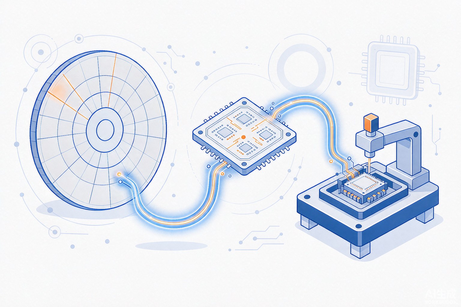
Programming service: firmware and data flashing for MCUs, Flash and EEPROM devices, supporting both pre-packaging wafer-level and post-packaging unit-level delivery. Every unit is verified by readback to ensure data integrity; programming data is handled under isolated controls to meet customer confidentiality requirements. Device types, programming methods and delivery flows can be tailored per project.
Get Tech Support
Tell us what you need — our engineering team will get back to you shortly.
Contact us