

Are power electronics engineers facing the dual challenges of complex high-frequency circuit design and energy efficiency bottlenecks in mid- to low-frequency systems?
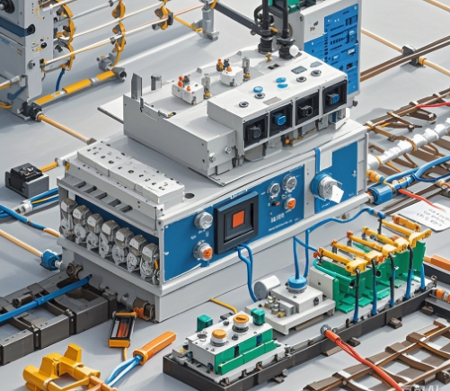
High switching frequency brings efficiency and size benefits — and also drive, layout and EMI complexity — while mid- to low-frequency high-power systems are capped by conduction loss. This article breaks down both challenges and shows how SiC MOSFETs address them.
Challenge One: Design Complexity at High Frequency
Raising the switching frequency from 16kHz to 50kHz and beyond delivers immediate efficiency and passive-component size benefits, but design complexity rises in step: gate-drive loops need lower inductance and stronger drive capability; every millimeter of power-loop inductance produces voltage spikes under high di/dt; the EMI spectrum shifts upward, increasing filtering and shielding cost; and heat is concentrated into a smaller area, making thermal design harder. This is why many engineers "want high frequency but dare not use it".
Challenge Two: The Efficiency Ceiling at Mid/Low Frequency
Conversely, in low-frequency high-power systems, switching loss becomes secondary and conduction loss dominates. Silicon IGBTs carry a 1.5–2.5V saturation voltage plus a tail current at turn-off; in motor drives and inverters running around the clock, that loss turns directly into heat and electricity cost. With conventional silicon devices, pushing efficiency further is approaching a hard ceiling.
How SiC MOSFETs Address Both
Silicon carbide MOSFETs improve both fronts at once. First, on-resistance is low — our HSCM1200N series 1200V platform spans 11–80mΩ — cutting conduction loss well below a comparable IGBT at the same current. Second, fast switching with no tail current keeps switching loss low even at high frequency. In practice: mid/low-frequency systems gain efficiency simply by switching to SiC; high-frequency systems use SiC together with a laminated busbar and optimized gate drive to keep spikes and EMI under control.
Practical Recommendations
- Identify the dominant constraint first: efficiency gaps point to conduction loss (choose lower RDS(on)); size gaps point to higher switching frequency;
- Any move toward high frequency must be paired with layout work: laminated busbar, compact commutation loop, negative-voltage turn-off;
- Hybrid solutions (IGBT + SiC antiparallel diode) are a pragmatic transition for cost-sensitive designs;
- When unsure, start with 1.5–2x margin and converge with measured junction temperature and efficiency curves.