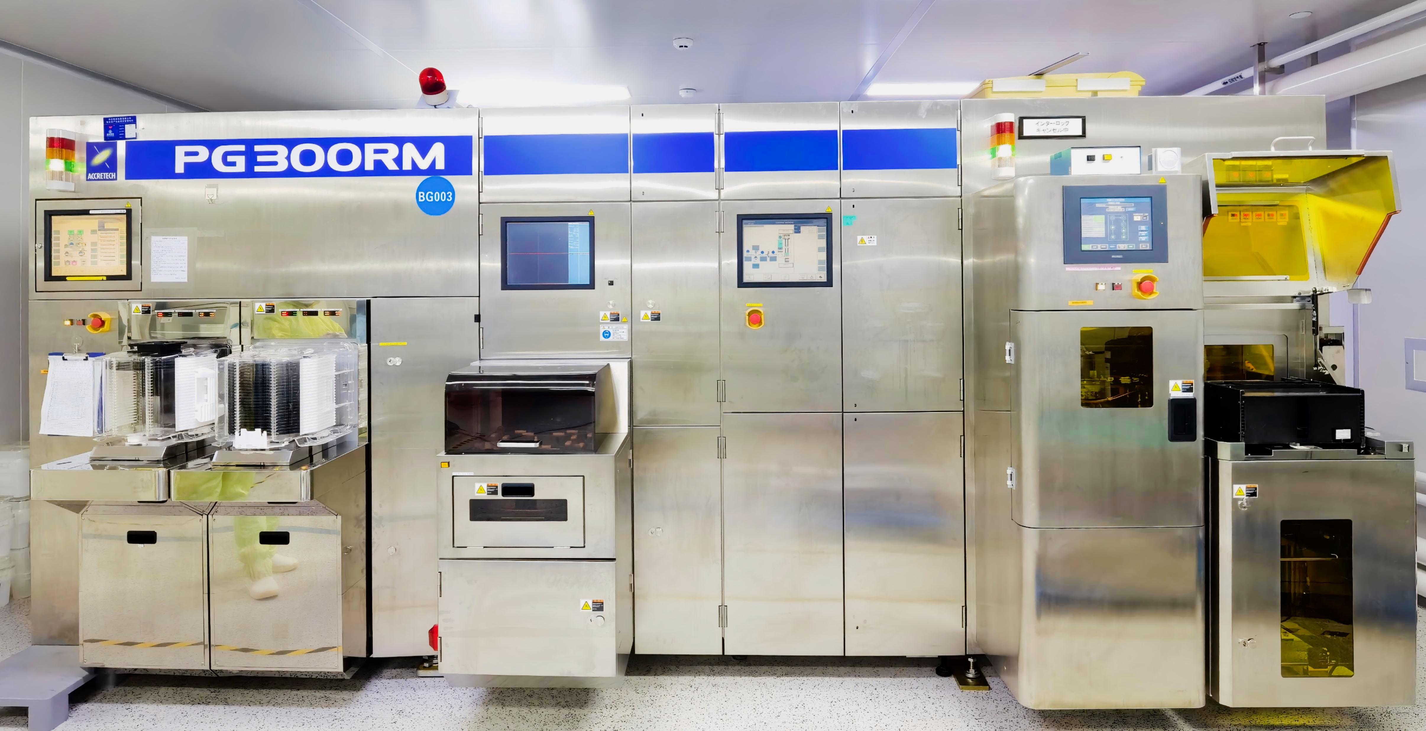
Wafer dicing & thinning
We process 6-inch, 8-inch and 12-inch wafers, with standard thinning thickness from 100 µm to 500 µm and ultra-thin capability (below 50 µm) available on request — meeting the most demanding advanced-packaging requirements.
1 articles
Wafer thinning and dicing decide the mechanical strength, packaging yield and final performance of finished chips. Hypersemi processes 6-inch, 8-inch and 12-inch wafers, with standard thinning from 100 µm to 500 µm and ultra-thin capability below 50 µm for the most demanding advanced-packaging requirements.
Process Capability
- Thinning — 100–500 µm standard window; below-50 µm ultra-thin on qualified requests.
- Dicing — street-width and chipping controlled to protect die strength.
- Handling — thin-wafer carriers and process recipes tuned per device type.
Where It Matters
Thinner dies mean lower thermal resistance and smaller packages; clean dicing means fewer cracks in molding and test. Both feed directly into your packaging yield — talk to us about your target thickness and die size before tape-out so the back-end window is designed in, not patched later.